What Are advance semiconductors and Why Do They Matter?
The electronics industry is transforming under the pressure of performance, efficiency, and time-to-market. advance semiconductors mark this turning point by uniting architectural innovation, advanced packaging, and smarter design workflows.
They enable new value in AI, cloud, automotive, and edge devices while tempering power use and system cost.
Modern supply chains and policy incentives are aligning to support scalable production without sacrificing reliability.
How Do Chiplet Architectures Redefine Modern Processors?
Monolithic dies struggle with yield, cost, and flexibility at leading nodes. Designers now disaggregate large functions into smaller tiles stitched together with ultra-fast links. This modular method lets teams mix compute, IO, and memory, shorten design cycles, and reuse proven IP blocks.
Leaders report better binning, higher effective yields, and the ability to customize SKUs for specific workloads—all while holding power in check with short on-package interconnects using advance semiconductors.
Chiplet ecosystems also encourage collaboration across foundries, OSATs, and IP vendors. Standardized die-to-die protocols and reticle-busting partitioning give architects room to scale performance beyond single-die limits.
This is one reason analysts call chiplets a durable pathway for long-term roadmaps built on advance semiconductors.
What Is 3D Packaging and Why Does It Matter Now?
Three-dimensional integration stacks components vertically to cut path length, boost bandwidth, and improve energy efficiency. Techniques such as hybrid bonding, TSVs, and wafer-level processes allow close coupling of compute and memory.
Thermal innovations—through-silicon heat paths, advanced TIMs, and localized micro-fluidics—keep temperatures in check as density rises with advance semiconductors.
3D integration complements chiplets: tiles can be placed side-by-side (2.5D) or stacked for ultra-short links. This synergy delivers higher system performance at practical cost, reinforcing the momentum behind advance semiconductors.
Which Companies Are Leading in Chiplets and 3D Packaging?
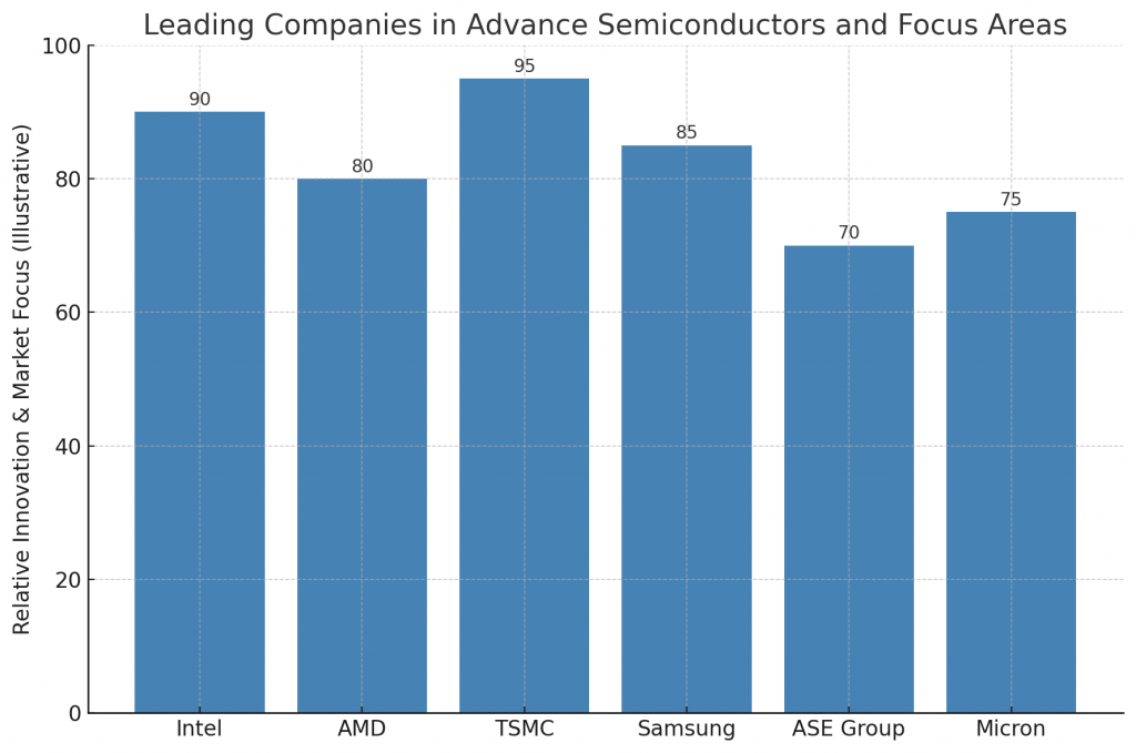
Global leaders are investing heavily in architectures, packaging, and manufacturing partnerships:
- Intel — EMIB, Foveros, and tile-based client/server CPUs targeting bandwidth and modularity.
- AMD — Multi-chip EPYC and Ryzen families proving performance gains from chiplet strategies.
- TSMC — Foundry leadership with CoWoS, SoIC, and hybrid bonding platforms for heterogeneous stacks.
- Samsung Electronics — 3D integration across memory and logic with advanced process nodes.
- ASE Group — OSAT expertise in high-density 2.5D/3D assembly and test.
- Micron — High-bandwidth memory and next-gen packaging for AI and HPC.
These roadmaps show how scaling will continue even as traditional transistor-level improvements slow, a core objective of advance semiconductors.
Strategic alliances and long-term offtake commitments are now common mechanisms to de-risk supply for programs centered on advance semiconductors.
Which Startups Are Transforming the Semiconductor Frontier?
Venture-backed companies are pushing specialized compute and novel packaging concepts:
- Tenstorrent — AI processors exploring modular chip fabrics.
- SiFive — RISC-V IP and configurable cores for flexible SoCs.
- Cerebras Systems — Wafer-scale engines for extreme training workloads.
- Graphcore — Intelligence processing units with innovative memory hierarchies.
- Lightmatter — Photonic acceleration for bandwidth-bound problems.
They prototype aggressively, then partner with foundries and OSATs to scale. This dynamic keeps pressure on incumbents to adopt open interconnects and faster release cycles aligned with advance semiconductors.
What Do Patents and TRL Levels Reveal About Maturity?
Patent clusters highlight hot zones: die-to-die PHYs, hybrid bonding flows, thermal interfaces, and memory-logic stacking.
Technology Readiness Levels indicate where risk is lowest:
- Chiplets: TRL 8–9 with broad commercial deployment in server and client CPUs.
- 3D Packaging: TRL 7–8 across mobile, AI, and networking parts.
- Photonic compute: TRL 4–5 with active pilots, promising but early.
When portfolio density and TRL alignment converge, commercialization accelerates—a pattern repeatedly observed in programs tied to advance semiconductors.
These signals help executives prioritize roadmaps and investment where outcomes are most predictable with advance semiconductors.
Where Do These Technologies Create the Biggest Impact?
Adoption spans many markets:
- Artificial Intelligence: High-bandwidth links and stacked memory for training and inference.
- Cloud Computing: Energy-efficient servers reduce total cost of ownership.
- 5G/6G Networks: Low-latency, power-aware baseband and radio units.
- Autonomous Systems: Real-time perception and decision pipelines at the edge.
- Healthcare & Life Sciences: Fast imaging, diagnostics, and genomics analytics.
- Defense & Aerospace: Radiation-tolerant packaging and secure compute.
Each case demands more bandwidth, tighter latency, and careful thermal design—areas where chiplets and vertical integration shine for programs built on advance semiconductors.
As design kits mature, solution providers offer pre-validated stacks that shorten time-to-value for advance semiconductors.
What Are the Hardest Challenges Right Now?
- Manufacturing complexity: Heterogeneous stacking and precise alignment add process steps.
- Thermal density: Vertical layers require advanced heat removal strategies.
- Test & yield: New failure modes demand improved DFT and known-good-die flows.
- Standards: Universal chiplet interfaces are emerging but not yet ubiquitous.
- Supply risk: Geographic concentration of fabs and packaging hubs creates exposure.
Mitigation revolves around co-design across silicon, package, and system; earlier thermal modeling; and shared standards for interoperability.
Teams that institutionalize these practices scale faster and unlock better cost curves for advance semiconductors, while reducing schedule risk for products powered by advance semiconductors.
What Is the Near-, Mid-, and Long-Term Outlook?
- 1–3 years: Wider chiplet use in client CPUs, AI accelerators, and networking silicon.
- 3–5 years: Broader 3D memory-logic stacks with mature thermal solutions.
- 5–10 years: Hybrid electronic-photonic subsystems and advanced materials.
Tooling, supply agreements, and standard IP blocks will make integration routine. The result is faster iteration cycles, more SKUs, and better unit economics across segments influenced by advance semiconductors.
As roadmaps converge on modular design, ecosystems will reward partners who prove reliability and deliver interoperable tiles for advance semiconductors.
How Can PatentsKart Help Semiconductor Teams Win Faster?
PatentsKart provides strategy and execution support from discovery to deployment:
- Patent landscapes & white-space maps to focus R&D and avoid crowded zones.
- Freedom-to-operate for priority markets to de-risk launches.
- Competitor & startup tracking across packaging nodes and interconnect IP.
- TRL-aligned roadmaps connecting lab milestones to product gates.
- Licensing & JV support to accelerate access to critical technologies.
With tailored research and actionable recommendations, we help clients convert complex options into clear decisions, compress time-to-market, and protect differentiation for advance semiconductors.
Our cross-industry perspective keeps you ahead of policy shifts, standards, and partner dynamics that can make or break programs based on advance semiconductors.
Conclusion
The shift to modular, vertically integrated systems is not a passing trend—it is the framework for the next decade of compute.
By embracing chiplets, stacking, and rigorous thermal and test methodologies, engineering teams deliver more performance within real-world power and cost envelopes.
With the right partnerships, processes, and protections in place, organizations can scale roadmaps confidently and set the pace for a new generation of products that benefit from advance semiconductors.
FAQs
Q1. What are the core ideas behind modern disaggregation?
Breaking a monolithic design into tiles improves yield, flexibility, and cost while enabling short, fast interconnects on package using standard protocols tied to advance semiconductors.
Q2. Which companies lead today?
Intel, AMD, TSMC, Samsung, ASE Group, and Micron drive roadmaps, with vibrant startups pushing specialized compute and packaging concepts.
Q3. Where do these approaches help the most right now?
AI training and inference, cloud computing, advanced networking, autonomous systems, and high-throughput analytics benefit first due to bandwidth and power constraints.
Q4. What slows adoption?
Manufacturing complexity, thermal density, evolving standards, and concentrated supply chains—each addressable with co-design, better DFT, and resilient sourcing.
Q5. How does PatentsKart reduce risk and speed execution?
We align patents, FTO, and TRL progress with partner and supplier choices so teams move from pilot to production on schedule and on budget.